Intel Unveils the World’s Thinnest Gallium Nitride (GaN) Chiplet
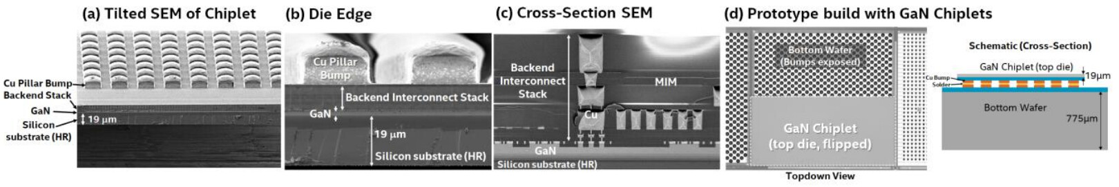
Intel Foundry has achieved a significant milestone in semiconductor innovation with the introduction of the world’s thinnest gallium nitride (GaN) chiplet. The base silicon layer of this chiplet measures just 19 micrometers in thickness, setting a new benchmark for compact, high-performance chip design.
Breakthrough GaN-on-Silicon Integration
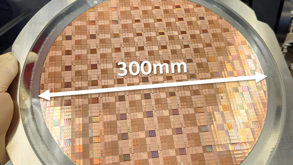
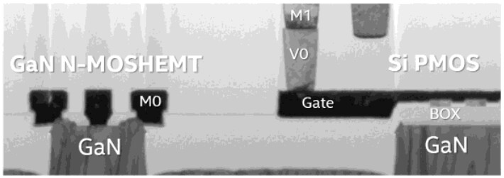
In a pioneering move, Intel has successfully manufactured a 300-millimeter GaN-on-silicon wafer, marking one of the first instances where gallium nitride is combined with traditional silicon logic on a single chip. Historically, GaN has been utilized primarily in power electronics, while silicon has remained the standard for computational logic. Intel’s innovation bridges this gap, enabling GaN semiconductors to handle power delivery and basic computational tasks within the same chiplet. This integration eliminates the need for separate chips to manage power and logic, streamlining system architecture and improving efficiency.
Advanced Manufacturing on the 30 nm Process
The GaN wafer was produced using a 30 nm process, resulting in impressive electrical characteristics. The chiplet demonstrates stable current carrying capabilities, minimal power loss, and can block voltages up to 78 volts without leakage. These features are particularly valuable for applications requiring high reliability and efficiency.
Superior Performance for Demanding Applications
Gallium nitride is renowned for its wide bandgap properties, supporting high-frequency performance that exceeds 300 GHz. Its superior material characteristics allow for efficient power delivery and stable operation at elevated temperatures. This makes the technology especially relevant for environments such as electric vehicles and data centers, where space constraints, high temperatures (up to 150°C), and operational stability are critical.
Comprehensive Logic Circuit Integration
Intel’s GaN-on-silicon chiplet incorporates a range of traditional logic elements, including inverters, NAND gates, multiplexers, and ring oscillators. Extensive testing has confirmed that these circuits meet the latest industry standards, achieving rapid switching times of just 33 picoseconds (33 trillionths of a second) consistently across the entire 300 mm wafer.
Implications for Future Technologies
This breakthrough in GaN and silicon integration demonstrates promising electrical performance, high yield, and scalability. As Intel continues to refine this technology, it holds significant potential for widespread adoption in robotics, AI data centers, and other advanced computing applications. The ability to combine power delivery and computational logic in a single, ultra-thin chiplet could redefine the design and efficiency of next-generation electronic systems.