Intel Launches 18A Process Node and Expands Arizona Manufacturing
Intel has made significant strides in semiconductor manufacturing with the introduction of its advanced 18A process node. According to industry reports, Intel began limited shipments of 18A wafers to U.S. customers in the third quarter, with full-scale production already underway. The company is set to unveil its first in-house 18A processor, codenamed Panther Lake, during its inaugural Tech Tour in Arizona on October 9. The Panther Lake AI PC chip is expected to ship by the end of the year, marking a major milestone in Intel’s roadmap for next-generation CPUs.
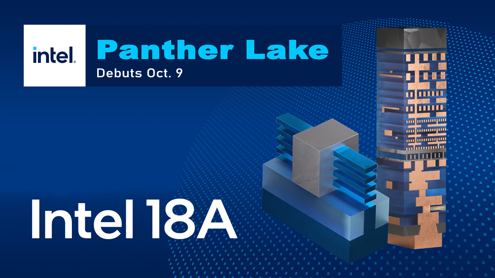
The 18A process node is a cornerstone for Intel’s upcoming CPU generations, supporting innovations that set new industry standards. Notably, Intel is the first foundry to bring backside power delivery to market, a breakthrough that reduces routing congestion and enhances frequency performance. This advancement positions Intel’s Arizona fabrication facilities as the first in the United States to achieve mass production at the 2 nm-class node.
Arizona Fab Expansion and Industry Impact
Intel’s expansion in Arizona, which includes Fab 52 and Fab 62, is the result of a $32 billion investment initiated in 2021. Fab 52 is projected to reach a monthly output of 1,000 to 5,000 wafers by the end of the year, ramping up to 15,000 wafers per month in 2026 and eventually scaling to 30,000. These facilities are becoming increasingly attractive to global chipmakers, especially in light of evolving U.S. chip tariff policies.
While the 18A node may not lead in transistor density, its innovative backside power delivery technology offers significant performance benefits. This approach, combined with Intel’s RibbonFET gate-all-around (GAA) architecture, delivers a reported 15% improvement in performance per watt and a 30% increase in chip density compared to previous generations. These enhancements are drawing attention from major technology companies worldwide.
Technological Innovations: PowerVia, RibbonFET, and Advanced Packaging
The 18A process represents Intel’s most significant transistor innovation since the introduction of FinFET technology in 2011. PowerVia, Intel’s proprietary backside power delivery system, works in tandem with RibbonFET GAA transistors to optimize both performance and energy efficiency. This combination is designed to meet the growing demands of AI, data center, and high-performance computing applications.
Looking ahead, Intel’s server CPU, Clearwater Forest, will also leverage the 18A process and is scheduled for release in the first half of 2026. This launch will coincide with the debut of Intel’s next-generation Foveros Direct 3D advanced packaging technology. In the realm of advanced packaging, Intel is focusing on two primary solutions: Foveros, which enables 3D chip stacking, and EMIB (Embedded Multi-die Interconnect Bridge). EMIB utilizes embedded silicon bridges at the die edges, offering greater packaging flexibility and reduced costs compared to traditional large-area interposer solutions like CoWoS.
With these advancements, Intel is reinforcing its leadership in semiconductor manufacturing, setting the stage for the next era of high-performance, energy-efficient computing.