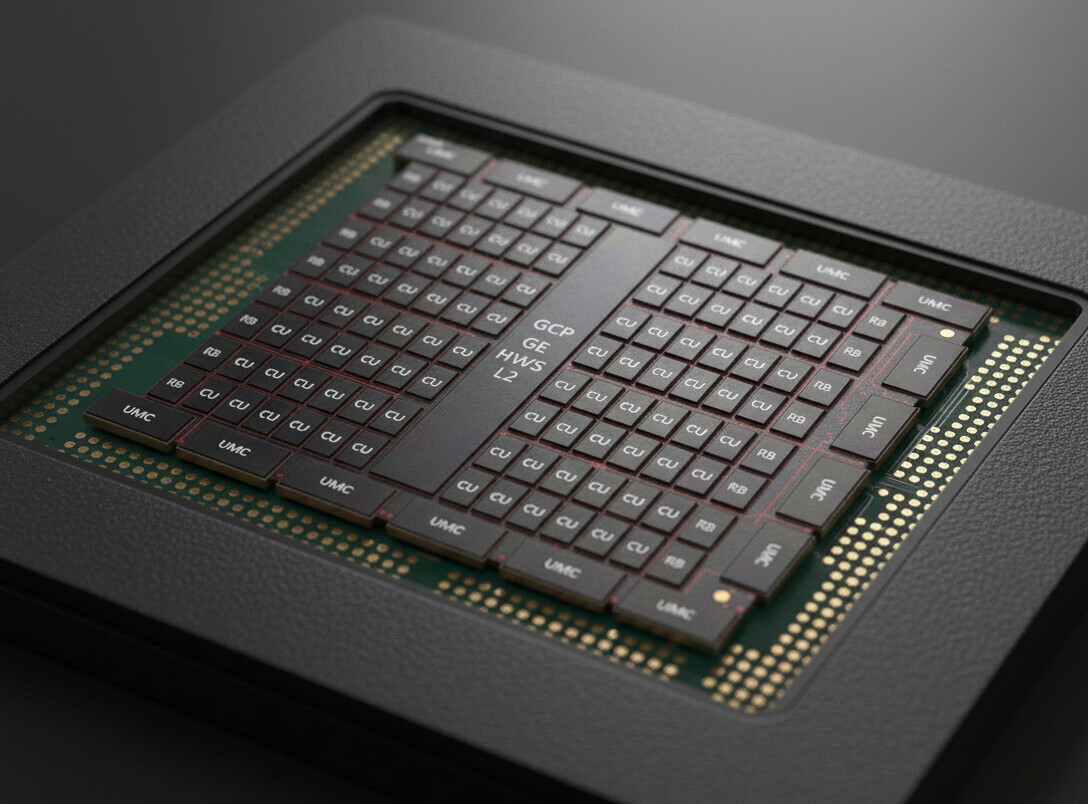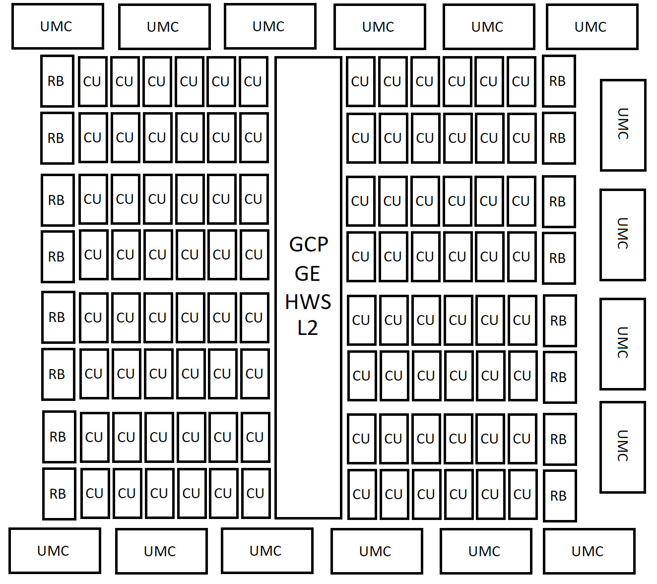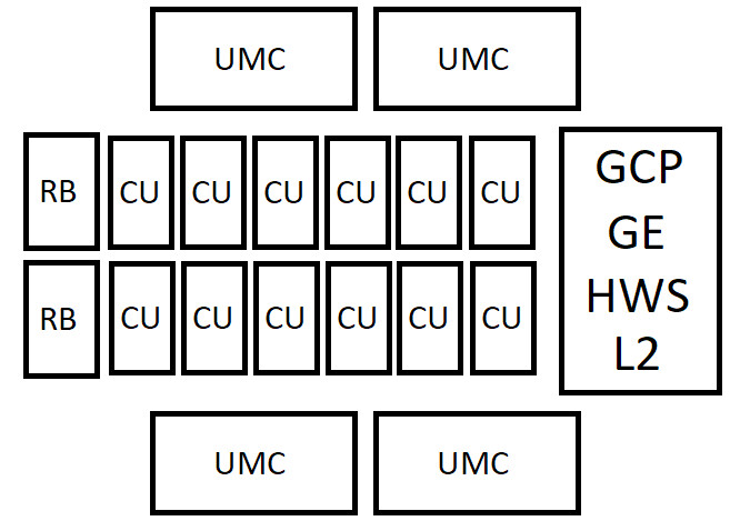
New diagrams released by a well-known hardware leaker @Kepler_L2 depict a highly modular AMD UDNA family that may consist of four different die sizes, with the largest potentially featuring 96 compute units. The illustrations showcase repeating shader arrays and shader engines, with each engine housing a few compute units and its own render backend. These engines then connect to a central SoC block that includes the graphics command processor, graphics engine, hardware schedulers, and a shared L2 cache. On the memory side, the flagship diagram displays sixteen unified memory controllers, each with 32 bits, resulting in a 512-bit external interface. The leak also suggests the presence of a significantly larger on-die Infinity Cache for the top-tier model.
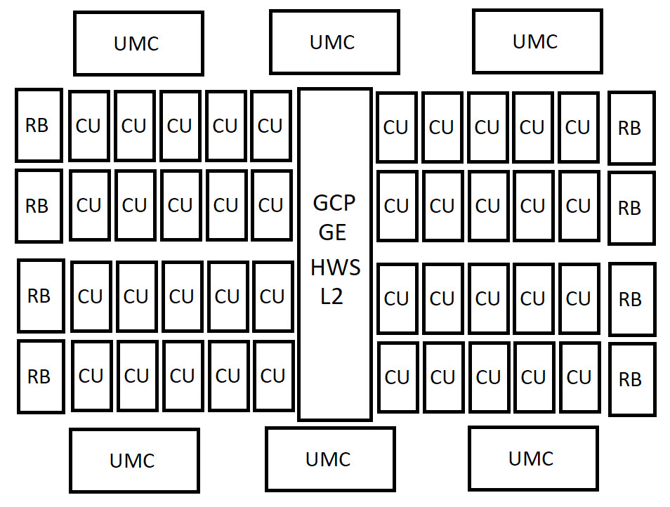
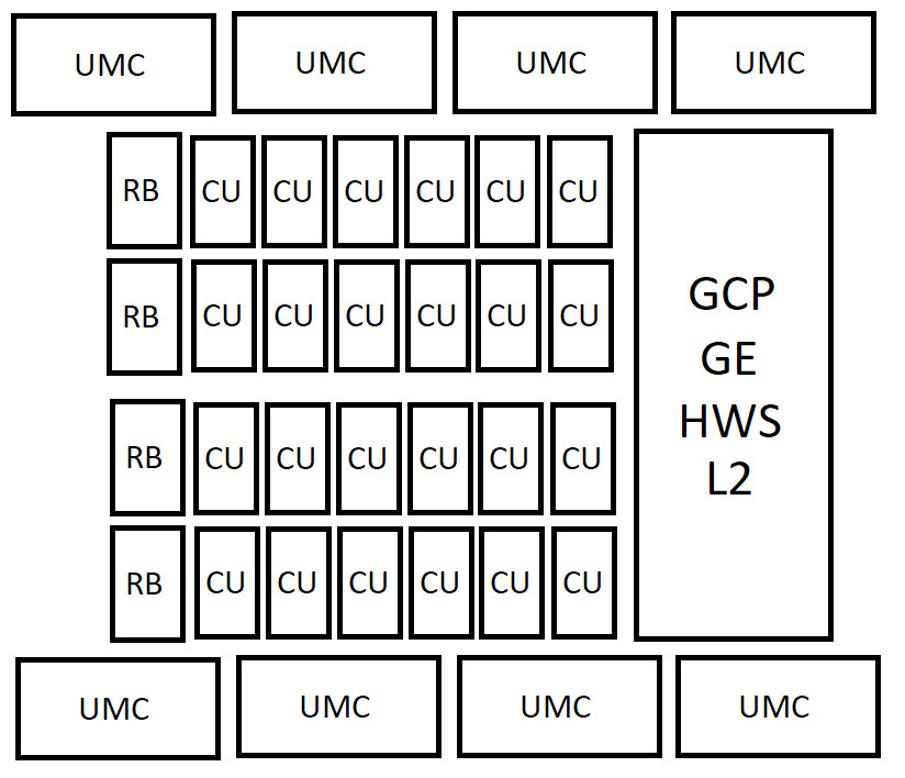
When the components are analyzed together, the flagship model's specifications align with the diagram. Eight shader arrays with two shader engines each amount to 16 shader engines, and with six compute units per engine, the total reaches 96 CUs. The mid-tier design scales back slightly, featuring four shader arrays and eight shader engines, with five compute units per engine, totaling around 40 compute units and an estimated six memory controllers for a 192-bit bus. Below that, there are 24 CU and 12 CU configurations constructed from smaller arrays and fewer controllers. The 24 CU design is depicted with up to eight memory controllers, suggesting potential variations in controller widths depending on the type of interface used.
Additional details in the diagrams go beyond just compute counts and bus widths. Notably, there is a hint that certain data-center-focused models could have larger per-CU local caches. The documents also suggest a convergence of Radeon and Instinct features under the UDNA branding, allowing AMD to utilize the same components for gaming, AI, or accelerator applications. This modular SoC design would enable flexibility in mixing and matching engine counts, cache sizes, and memory controller configurations across a single product family. It is important to note that these details are unofficial and speculative. While the diagrams propose a feasible approach for AMD to scale a single architecture, they do not confirm that the silicon has been finalized or that specifications are set in stone. AMD still has the ability to adjust CU counts, memory widths, cache sizes, or SKU names before production commences.